
Products
Semiconductor Optics
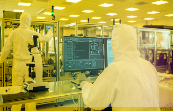
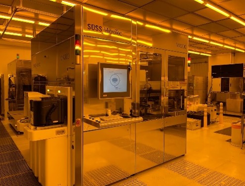
Lithography Process Foundry
Feature
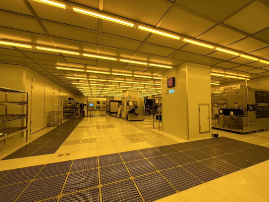
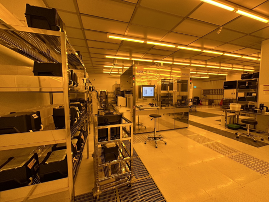
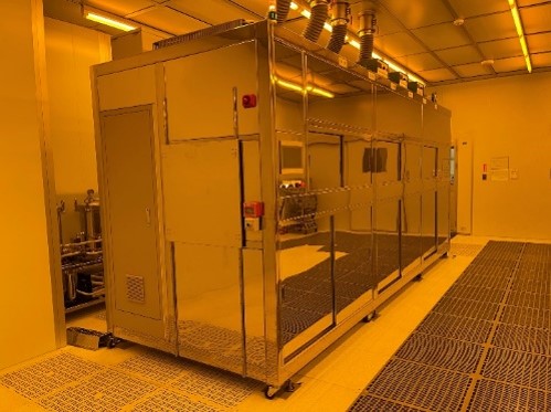
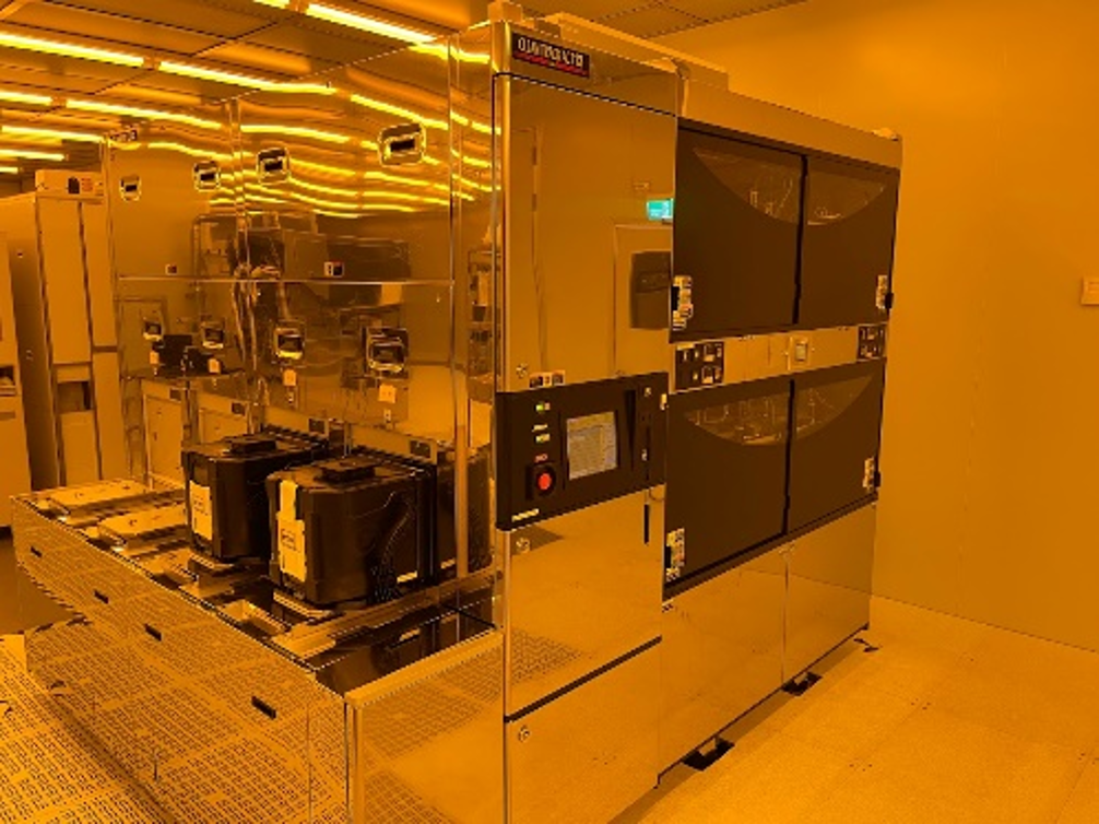
MOE can provide a complete set of professional lithography process, including spin-coating, exposure, develop, and photoresist strip . The applicable range of wafer size is 6" 8" 12"
•1. 6", 8", 12" Semiconductor optical foundry
•2. 8", 12" Photoresist, etching foundry